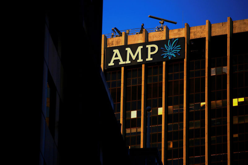
Australia’s AMP said on Friday it would sell its infrastructure debt platform to Ares Management for A$428 million ($310 million) as part of its strategy to simplify its private markets business ahead of a spin-off next year.
The 172-year-old company is trying to restore its reputation and reorganise itself into a simpler outfit, as it continues to lose clients after years of scandals involving employees, regulators and customers.
AMP said the deal would result in Los Angeles-based Ares gaining the debt platform’s A$7 billion in invested assets under management and its entire investment team.
The embattled wealth manager had failed to sell its asset management arm’s private markets business this year, instead opting to spin off and re-brand the unit.
In February, Ares withdrew an A$6 billion offer for the wealth manager in a setback for AMP, which has been embroiled in recent years in controversies.
They include allegations of sexual harassment, lying to regulators and charging customers fees for services it never provided.
AMP’s misconduct led to the resignation in 2018 of former chairman Catherine Brenner and chief executive Craig Meller.
The demerger is on track to complete late in the first half of 2022, AMP said on Friday.
- Reuters with additional editing by George Russell
READ MORE:
CEO Brett Cairns Resigns at Australia’s Magellan: The Age
Singtel Flags $216m Exposure in Australia Tax Case Defeat
Caroline Kennedy Nominated as US Envoy to Australia